USB bus power supply |
4.0 to 5.25V |
---|---|
Self-powered |
3.0 to 3.6V |
I/O voltage: |
1.8V to VDD |
Operating temperature |
-40 ° C ~ 85 ° C |
Shipping Weight | 0.01 kg |
Shipping Dimensions | 5 × 5 × 1 cm |
CP2112 debug board USB to I2C Communication Module
- On-chip power-on reset circuit, on-chip voltage regulator: 3.45 V output
- Compliant with USB specification 2.0 standard; full speed (12Mbps)
- USB suspend status via SUSPEND and /SUSPEND pins
- Integrated 194-byte one-time programmable ROM for storing customizable product information
₨ 1,570.00
Out of stock
Out of stock
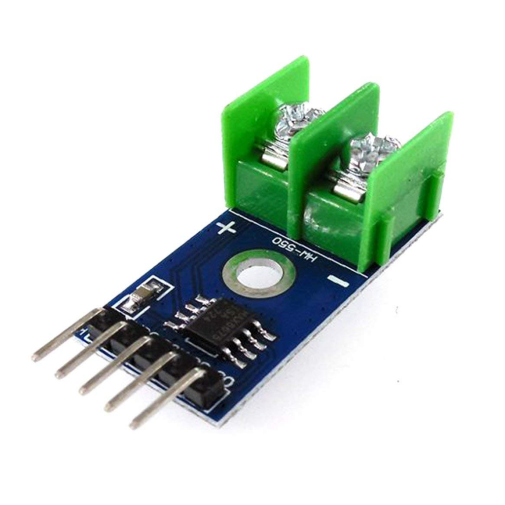
This is a CP2112 debug board USB to I2C Communication Module.
The CP2112’s highly integrated USB-to-SMBus bridge controller integrates a USB 2.0 full-speed function controller, USB transceiver oscillator and eight GPIO pins. All customization and configuration options can be selected through a simple GUI-based configurator. Standard HID class devices do not require the development of complex firmware and drivers. The CP2112 device enables fast USB connectivity with minimal development effort.
The CP2112 uses the standard USB HID device class, which is natively supported by most operating systems. A custom driver does not need to be installed for this device. Host applications communicate with the CP2112 through interface libraries provided by Silicon Labs. The interface specification for the CP2112 is also available to enable the development of an API for any operating system that supports HID.
The CP2112 SMBus interface includes the SDA and SCL signals needed for SMBus communication and is configurable. The configurable options include the clock speed, read/write timeouts, retry counter timeout, SCL low timeouts, and a 7-bit device address. The CP2112 will only ACK the 7-bit device address assigned to it but will not respond to any read/write requests. External pull-up resistors are needed for the SCL and SDA signals.
The device also features a total of eight GPIO signals. The GPIO signals are controlled through USB and can be configured as Input/ Output and Open-Drain/Push-Pull. Three of the GPIO signals support alternate features including a configurable clock output (48 MHz
to 94 kHz) and TX and RX LED toggle. Support for I/O interface voltages down to 1.8 V is provided via a VIO pin.
Features:
- On-chip power-on reset circuit, on-chip voltage regulator: 3.45 V output
- Compliant with USB specification 2.0 standard; full speed (12Mbps)
- USB suspend status via SUSPEND and /SUSPEND pins
- Integrated 194-byte one-time programmable ROM for storing customizable product information
- 512-byte SMBus data buffer, configurable clock speed device address 7-bit value is the slave address of CP2112
- Windows, Mac, and Linux HID to SMBus libraries API for rapid application development, open-access interface specifications.
- 8 GPIOs can be configured as input/output and open-drain/push-pull, configurable clock output for external devices 48MHz to 94kHz, switching LEDs during read/write SMBus
- Module size: 29.5mm*21.3mm, with two M3 mounting holes, one MicroUSB female port
- Application areas: Portable controllers, USB dongle, data logging
Package Includes:
1 x CP2112 debug board USB to an I2C communication module
Only logged in customers who have purchased this product may leave a review.
Reviews
Clear filtersThere are no reviews yet.