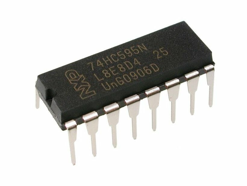
The 74HC595 is a high-speed CMOS Shift Register with an 8-bit serial-in, parallel-out shift register and storage register. Here?s a detailed overview of its features and applications:
### Key Features:
1. **8-bit Serial-in, Parallel-out Shift Register**: Converts serial data input to parallel data output.
2. **Storage Register with 3-state Outputs**: The parallel output can be set or reset to store data.
3. **Clock Inputs**: Two clocks (Shift Register Clock and Storage Register Clock) allow independent control of the shift register and the storage register.
4. **Latch Enable (LE) Input**: Allows the transfer of data from the shift register to the storage register.
5. **Output Enable (OE) Input**: Enables or disables the output buffers.
6. **High-speed Operation**: Typical maximum clock frequency is 100 MHz.
7. **Wide Operating Voltage Range**: Typically 2V to 6V.
8. **Low Power Consumption**: CMOS technology ensures minimal power usage.
### Pin Configuration:
1. **Q0-Q7 (Pins 15, 1-7)**: Parallel outputs.
2. **DS (Pin 14)**: Serial data input.
3. **OE (Pin 13)**: Output enable input (active low).
4. **MR (Pin 10)**: Master reset input (active low).
5. **SHCP (Pin 11)**: Shift register clock input.
6. **STCP (Pin 12)**: Storage register clock input.
7. **Vcc (Pin 16)**: Supply voltage.
8. **GND (Pin 8)**: Ground.
### Applications:
1. **LED Display Drivers**: Commonly used to control LED matrices and segment displays.
2. **Data Bus Expansion**: Expands the number of I/O pins available in microcontroller projects.
3. **Signal Routing**: Utilized in various signal routing applications in digital circuits.
4. **Keypad Controllers**: Manages multiple keypad inputs and outputs.
5. **General Purpose Logic**: Suitable for general-purpose digital logic applications requiring serial-to-parallel data conversion.
### Basic Operation:
1. **Serial Data Input**: Data is fed serially into the DS pin.
2. **Clocking Data**: On each rising edge of the SHCP clock, the data is shifted into the register.
3. **Latching Data**: When the STCP clock is triggered, the data in the shift register is latched into the storage register.
4. **Output Enable**: If OE is low, the latched data is presented on the output pins Q0-Q7.
### Example Circuit:
To drive an LED display:
– Connect DS to a microcontroller’s data output pin.
– SHCP and STCP connected to microcontroller’s clock and latch pins, respectively.
– OE and MR connected to GND (for always enabled output and no reset).
– LEDs connected to Q0-Q7 through current limiting resistors.


Reviews
Clear filtersThere are no reviews yet.